@lunar
2016-05-23T17:59:46.000000Z
字数 5854
阅读 3194
Catalog
Ⅰ. Abstract
In this report we will show how to reduce the volume of summation of chips used in the watch. Firstly, some short introductions of each single component will be given. And then, we will explain the exactly method to finish the task and the rules which need to obey. Finally, the overall circuit diagram is provided with reference at the end.
Ⅱ . Single Component Introduction
① ATmega328P
ATmega328P is a 8-bit Microcontroller with 32KBytes in-system programmable flash, and the most important control&compute component.
1.Pin Descriptions
This part is a brief introduction of the ports we will use in our project.
- VCC
Digital supply voltage. - GND
Ground. - Port C(PC5:0)
Port C is a 7-bit bi-directional I/O port with internal pull-up resistors.The PC5...0 output buffers have symmetrical drive characteristics with both high sink and source capability. - AVcc
AVcc is the supply voltage pin for the A/D Converter, PC3:0, and ADC7:6. - AREF
AREF is the analog reference pin for the A/D Converter.
2.Overview
Basically, the chip we use (ATmega328P) is a low-power CMOS 8-bit Microcontroller based on the AVR enhanced RISC architecture. During each single clock cycle, the chip will execute powerful instructions so that it achieves throughputs approaching 1 MIPS per MHz to allow the designer of system to optimize power consumption versus processing speed.
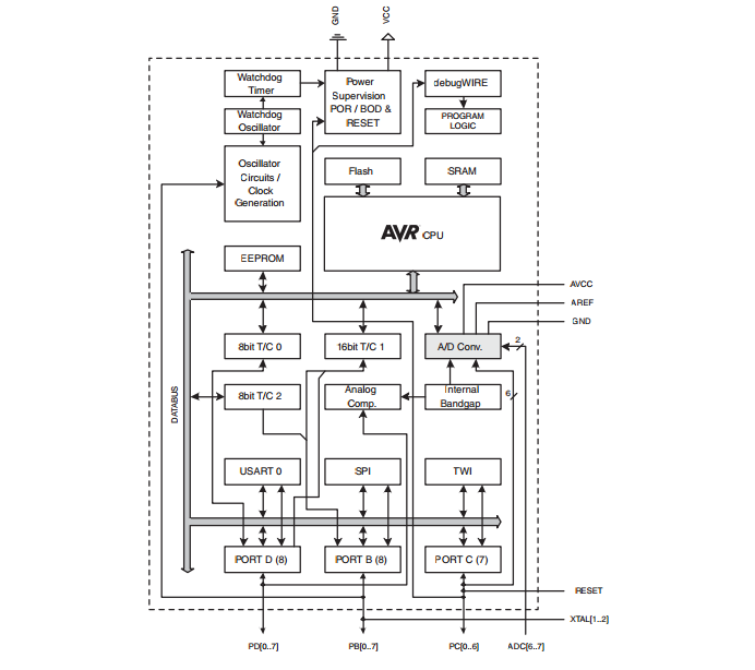
2.1 Block Diagram
2.2 Features
- Advanced RISC Architecture
- High Endurance Non-volatile Memory Segments
- Atmel QTouch library support
- One 16-nit Timer/Counter with Seperate Prescaler, Compare Mode, and Capture Mode
- Power-on Reset and Programmable Brown-out Detection
- 23 Programmable I/O Lines
- Operating Voltage : 1.8V - 5.5V
- Temperature Range : -40℃ to 85℃
- Speed Grade : 0 - 4MHz@1.8 - 5.5V, 0 - 10MHz@2.7 - 5.5V, 0 - 20MHz@4.5 - 5.5V
② TMP36
TMP36 is a low voltage temperature sensor.It can be used to detect current temperature.
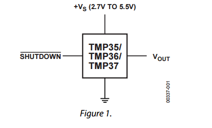
1.Pin Descriptions
-
From 2.7V to 5.5V -
Output voltage - GND
Ground - NC
No connection
2.Overview
TMP36 can read temperatures from -40℃ to +125℃ and provide a voltage output that is linearly proportional to the Celsius temperature.
2.1 Block Diagram
2.2 Features
- Low voltage operation : 2.7V to 5.5 V
- Calibrated ℃
- 10 mV/℃ scale factor
- Stable with large capacitive loads
- Less than 50 quiescent current
- Shutdown current 0.5 max
③ ESP8266
ESP8266 is a Wi-Fi module.
1.Pin Descriptions
- VCC
Power. - RST
Reset. - TXD
The TXD pin is the output from the module and is 3.3V logically. - RXD
The RXD pin is the input into the module and is 5V compliant. - GND
Ground.
2.Overview
We will use ESP8266 to add internet to our project.
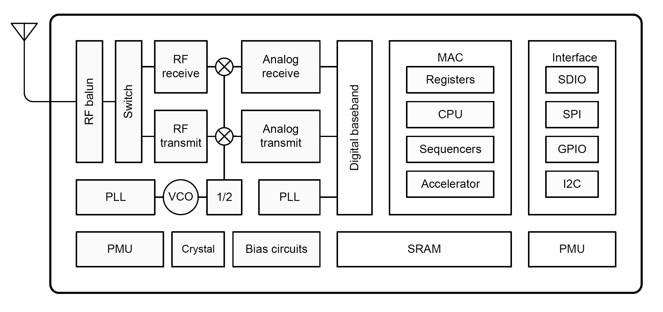
2.1 Block Diagram
2.2 Features
- 802.11 b/g/n
- Wi-Fi Direct(P2P), soft-AP
- Intergrated TCP/IP protocol stack
- Intergrated TR switch, balun, LNA, power amplifier and matching network
- Intergrated PLLs, regulators, DCXO and power management units
- +19.5dBm output power in 802.11b mode
- Power down leakage current of <10uA
- 1MB Flash Memory
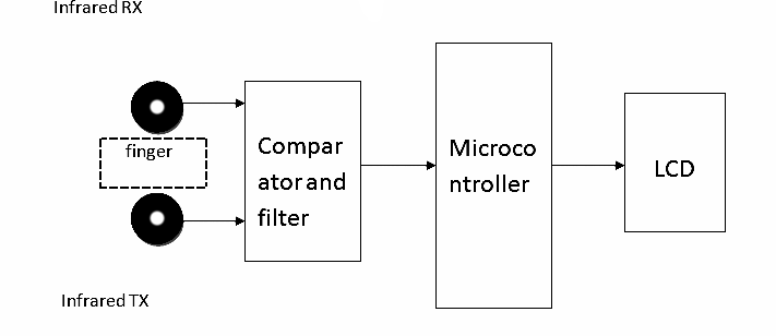
④ Pulse Sensor
Pulse Sensor is a well-designed plug-and-play heart-rate sensor.
1.Pin Descriptions
- VCC (Red)
3V to 5V - GND (BLACK)
Ground. - Signal (Purple)
2.Overview
The sensor clips onto a fingertip or earlobe and plugs right into Aeduino with some jumper cable.
2.1 Block Diagram
2.2 Features
- The refresh rate of raw Pulse Sensor signal : 2ms.
Ⅲ . Method to educe System's Size
A single-chip hardware circuit design application system usually consists of two parts:
Firstly, the system expansion, the microcontroller internal functional units, such as ROM, RAM, I/O, timer or counter, interrupt system, etc. If units above can not meet the requirements of the application system, the chip must be extended. The chip should be selected with the appropriate circuits design. Secondly, the configuration of the system, that is in accordance with the system functions required to configure peripheral devices, such as keyboards, monitors, printers, A/D and D/A converters, etc., to design appropriate interface circuits.
Expansion and configuration of the system should follow the following principles:
- As far as possible to choose a typical circuit, microcontroller and meet common usage. Lay a good foundation for standardized and modularized hardware systems.
- The configuration system expansion and peripheral levels should adequately meet the functional requirements of the application system, and leave appropriate room for secondary development.
- The hardware architecture should be put into consideration combined with application software solutions. Hardware architecture and software programs are likely to influence each other, considering the principle: Use the software functions which can be realized by the software as much as possible to simplify the hardware structure. It must be noted that by the software with hardware features, the general response time is longer than the hardware and CPU time.
- Ensure the related devices of the system possibly match with each other in performance. Such as the selection of CMOS chip microprocessor low-power system, in which all the chips are perfect for low-power products.
- Reliability and anti-jamming design are integral parts of the hardware design, which includes chips, device selection, decoupling filter, printed circuit board layout and channel isolation.
- When with massive single-chip peripheral circuits, remember to take into account their drive ability. With insufficient drive capability, the system will not work reliably. The bus load can be reduced through the addition lines to enhance drive capability or reducing chip power consumption.
- Try possibly towards the "one-chip" design direction hardware system. The more system components, mutual interference between the device and the stronger the power consumption also increases, inevitably reduce the stability of the system. With the microcontroller chip integration becoming more powerful, true system-on-chip SoC has been able ach, such as ST company recently launched μPSD32 ×× series on a single chip integrates a 80C32 core, high-capacity FLASH memory, SRAM, A/D convertor, I/O, two serial ports, watchdog, power-on reset circuit and so on.
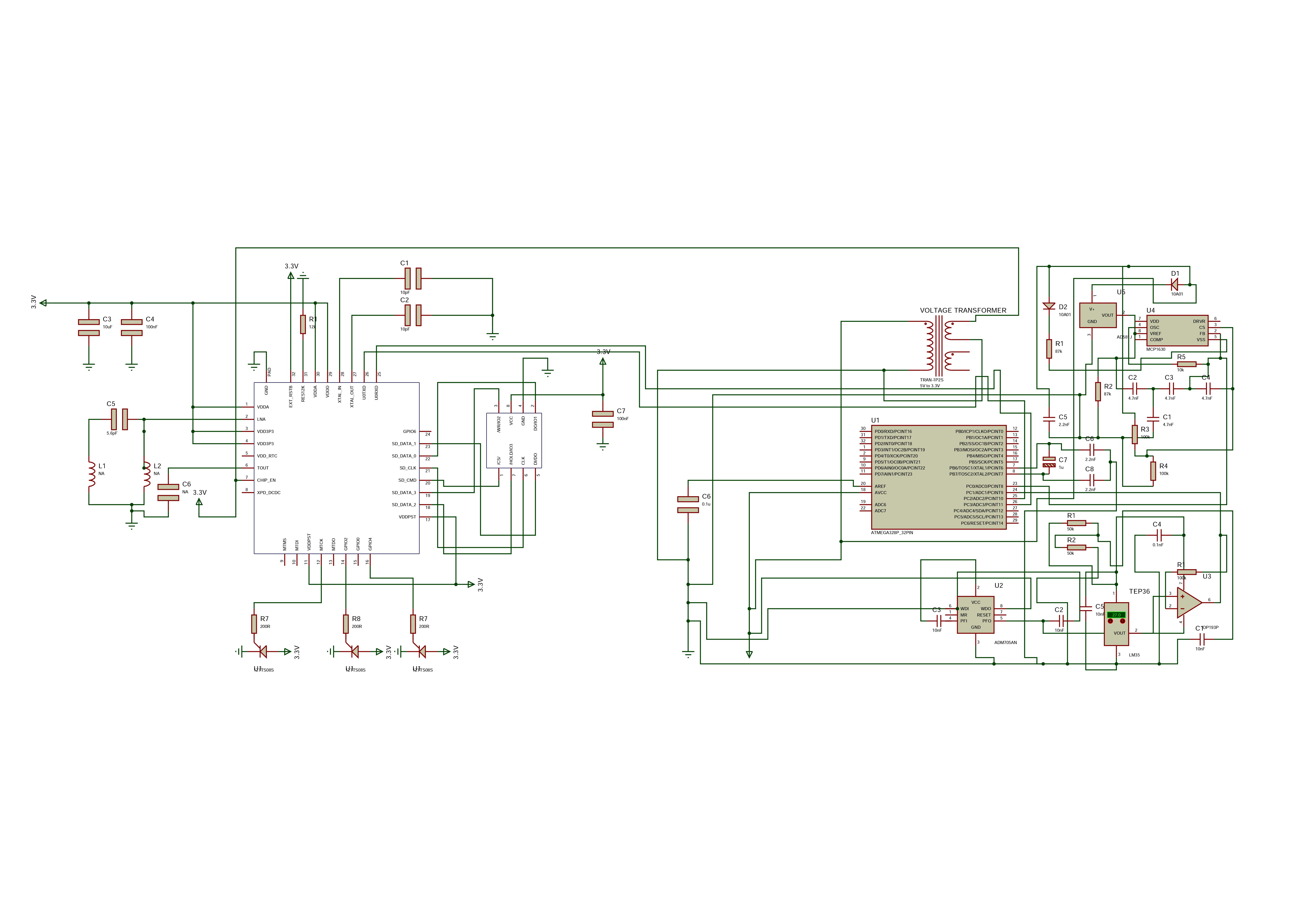
Ⅳ . Overall Circuit Schematic